Home/ Elements/ In
Indium
In 49

Indium

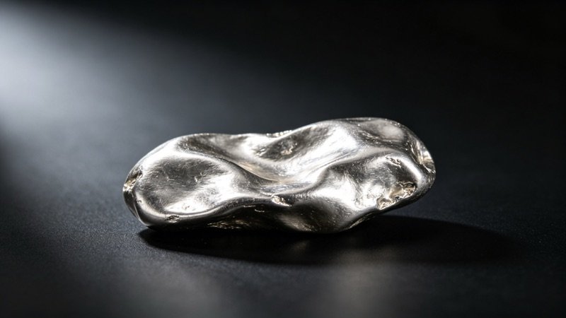
Indium is a chemical element; it has symbol In and atomic number 49. It is a soft silvery-white metallic element that makes up 0.21 parts per million of the Earth's crust, making it less abundant than silver. Indium was discovered in 1863 by German chemists Ferdinand Reich and Hieronymous Theodor Richter by spectroscopic methods. Indium is primarily used in indium tin oxide (ITO) transparent conductive coatings for touch screens, flat-panel displays, and solar cells. Other uses include low-melting-point alloys and semiconductors.

Post-transition Metal USGS 2025 silvery lustrous gray
Atomic number 49Z
Atomic mass 114.818u
Valence e⁻ 3
Electron config. 1s2 2s2 2p6 3s2 3p6 4s2 3d10 4p6 5s2 4d10 5p1
Density
7.31g/cm³
Melting point
157°C
Crustal abundance
0.25ppm
Annual production
1080metric tons unless otherwise specified
Recycling rate
10%(Low recycling rate (~10%); indium tin oxide (ITO) scrap from LCD screens)

Why This Element

Indium is the rarest element (0.25 ppm crustal abundance) with mass production and has historically been the most expensive metal per kilogram. Its primary industrial value stems from indium tin oxide (ITO) — the transparent conductive coating on nearly all touch screens, LCD, and OLED displays — where no substitute offers the same optical transparency combined with good electrical conductivity.

Applications

Touchscreen ITOSemiconductorsSolder

Applications in DepthElement & compound uses

Main Uses of the Element

Indium is a soft, low-melting, slightly bluish scattered (rare) metal. It has almost no independent ore deposits in the crust and is recovered entirely as a by-product of zinc and lead-zinc smelting, so output is small and price high. Its best-known use is in touchscreens and displays: indium tin oxide (ITO) transparent conductive films are the only transparent electrode material produced at large scale for flat-panel LCDs, OLEDs, touch panels, and plasma TVs. For any application requiring a material that is both transparent and conductive, almost no other material offers a comparable price-performance ratio; behind the screen glass of smartphones, tablets, laptops, and self-service terminals lies an ITO film only tens of nanometers thick. In semiconductors, compound semiconductors of indium with phosphorus and arsenic are key materials for infrared detection, fiber-optic communications, and high-frequency devices: indium phosphide is the substrate for lasers and detectors in long-haul fiber-optic communications, while indium arsenide is used in infrared sensors and terahertz devices. Soldering is another important market for indium: indium-based soft solders are low-melting, wet well, and buffer thermal stress between materials with different coefficients of thermal expansion, used in semiconductor packaging, low-temperature vacuum seals, and photovoltaic modules; they are especially irreplaceable in aerospace and cryogenic electronics that require extremely low-temperature joints. It is also used in low-melting alloys (fire sprinklers, fusible plugs), alloy bearings, and nuclear-radiation detectors.

Key Compounds and Their Uses

Indium sesquioxide (In2O3) is one of the main constituents of ITO transparent conductive films, a white or pale yellow powder; when doped with tin it becomes a conductive transparent film, the core electrode material for touchscreens, LCD panels, and OLED displays. Indium arsenide (InAs) is a narrow-bandgap semiconductor with extremely high electron mobility, used mainly to make infrared detectors, quantum-well devices, Hall sensors, and high-speed electronic devices, and in terahertz imaging research. Indium phosphide (InP) has a direct bandgap and high electron mobility and is the substrate material for 1310-nm and 1550-nm lasers, photodetectors, and high-speed HEMTs in fiber-optic communications, underpinning today's backbone internet optical networks. ITO, short for Indium Tin Oxide, is a solid solution of In2O3 doped with about 10% SnO2; it combines high transparency in the visible with high reflectance in the near infrared and, besides display electrodes, is used as low-emissivity glass, anti-icing heater films on aircraft, and transparent electromagnetic-shielding coatings.
Element History

Discovered in 1863 by Ferdinand Reich and Hieronymous Richter while analyzing sphalerite (zinc sulfide) ore from Saxony — they observed a new indigo spectral line and named the element accordingly. Isolated as pure metal shortly after. Production is entirely byproduct of zinc mining; approximately 60% of global production comes from China.

Alloys of this element (1)

View all alloys → InSb

Related Elements

Al · Aluminium Ga · Gallium Sn · Tin Tl · Thallium Pb · Lead Bi · Bismuth Po · Polonium Fl · Flerovium

Frequently Asked QuestionsLong-tail Q&A · data-driven

What is the melting point of Indium?
157 °C
What is the boiling point of Indium?
2072 °C
What is the density of Indium?
7.31 g/cm³
What are the atomic number and category of Indium?
49 · Post-transition Metal
Which ore is Indium mainly extracted from?
sphalerite (byproduct)
What are the world reserves of Indium?
1800 metric tons unless otherwise specified
What is the annual production of Indium?
1080 metric tons unless otherwise specified
What are the main uses of Indium?
Indium is the rarest element (0.25 ppm crustal abundance) with mass production and has historically been the most expensive metal per kilogram. Its primary industrial value stems from indium tin oxide (ITO) — the transpa
Who discovered Indium and when?
Ferdinand Reich · 1863